Written by Microscopehunt Authority
.

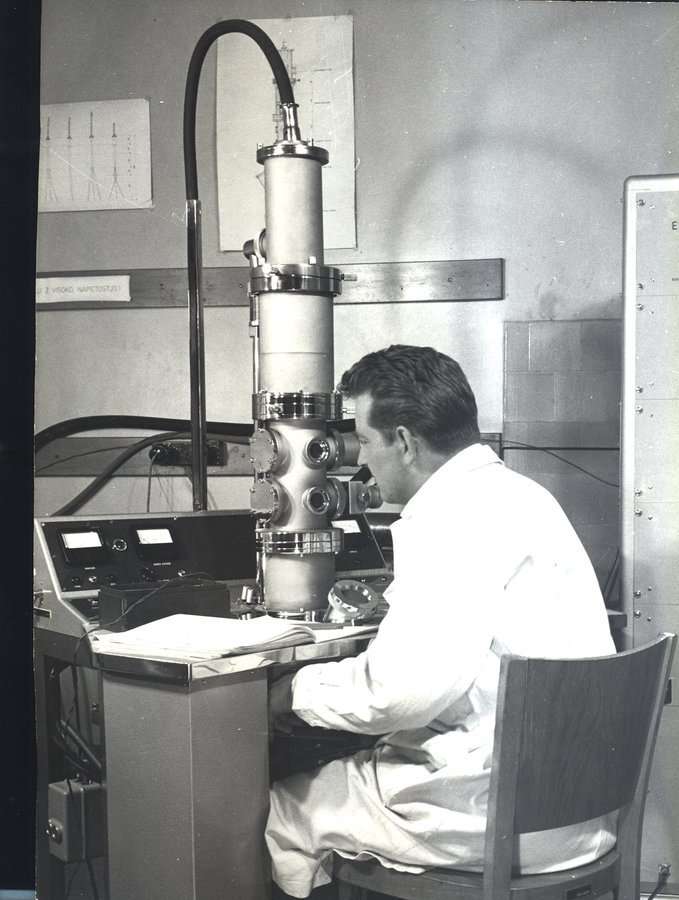
An electron microscope is a sophisticated instrument that uses a beam of accelerated electrons instead of light to create images of very small objects. This technology allows scientists to achieve much higher magnification and resolution than traditional light microscopes. The shorter wavelength of electrons enables researchers to view structures at the nanoscale, revealing details that are invisible to the naked eye or standard optical microscopes.
Types of Specimens Analyzed
Electron microscopes can investigate a diverse range of specimens. In the biological sciences, they are commonly used to study cells, tissues, and microorganisms. These microscopes are also valuable in materials science for examining metals, crystals, and complex materials. The ability to analyze both biological and inorganic samples makes electron microscopy an essential tool in various fields, including medicine, nanotechnology, and industrial quality control.
Interaction of Electron Beams with Specimens

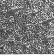
When the electron beam interacts with a specimen, it loses energy in various ways. This energy loss is transformed into different signals, such as secondary electrons and X-rays. Each type of signal carries unique information about the specimen’s surface and composition. For instance, secondary electrons help reveal the surface topography, while X-rays provide insights into the elemental composition. The scanning electron microscope (SEM) processes these signals to create detailed images, enabling in-depth analysis of the specimen.
Importance of Vacuum in Electron Microscopy
One critical requirement for using an electron microscope is that samples must be viewed in a vacuum. This is because air molecules can scatter the electrons, which would lead to poor image quality. By maintaining a vacuum around the specimen, the electron beam can travel without interference, resulting in clearer and more detailed images. Additionally, a vacuum environment helps prevent contamination and oxidation of the samples, further ensuring the accuracy of observations.
Challenges with Non-Conductive Materials

Imaging non-conductive materials can be challenging when using electron microscopes. Many electron microscopes are designed to work best with conductive specimens. Non-conductive materials, such as plastics or biological samples, can accumulate charge when exposed to the electron beam, leading to image distortion. This charge buildup can obscure details and reduce image quality. As a result, non-conductive specimens often require special preparation to be effectively imaged.
Preparing Non-Conductive Specimens
To prepare non-conductive materials for electron microscopy, several methods can be used. A common approach is to apply a thin conductive coating, such as gold or carbon, to the specimen. This coating minimizes charge buildup and enhances image quality. Some electron microscopes feature low-voltage settings that enable the imaging of non-conductive specimens without the need for coatings. Additionally, variable pressure or environmental scanning electron microscopes can analyze non-conductive materials without the need for special treatment.
Cost Comparison with Confocal Light Microscopes
Electron microscopes are generally more expensive to purchase and maintain than traditional light microscopes. However, the costs associated with confocal light microscopy have started to converge with those of basic electron microscopes. This shift means that researchers must carefully evaluate their specific requirements and budgets when selecting between these microscopy techniques. Each method offers unique benefits, and the decision will often depend on the particular applications and types of specimens being studied.
Conclusion
electron microscopes are vital tools for scientific research, providing detailed insights into the structures of various specimens. Their ability to produce high-resolution images makes them essential in both biological and industrial applications. Understanding how to prepare samples and the challenges of imaging non-conductive materials is crucial for effectively using these advanced instruments.
.
The Electron Microscope is a groundbreaking innovation that has transformed our ability to study the microscopic world. By using electron beams instead of light, it achieves unparalleled magnification and resolution, enabling researchers to explore structures at the nanoscale. This tool has been vital in fields like biology, materials science, nanotechnology, and medicine, allowing scientists to observe cellular structures, viruses, and atomic arrangements with extraordinary precision.
.
Despite challenges like high costs and complex operation, its contributions to scientific discovery are unmatched. The Electron Microscope continues to drive innovation, expanding the frontiers of knowledge and shaping the future of science and technology.
